
晶振官方博客
更多>>Ultra-small quartz crystal physical and electrical properties
來源:http://m.gajd.com.cn 作者:康華爾電子技術 2019年10月29
The physical and electrical properties of an ultra-small low profile quartz crystal oscillator and their production methods are described below.
AT-cut quartz crystal resonators have been used in precision frequency control products for more than 60 years and today are among the most widely used crystal types. Although conventional AT crystals are disc shaped, the need for smaller components has led to the development of micro AT stripes. To meet manufacturers' needs for smaller components, Statek Corporation has developed ultra-small low profile, thin quartz crystals as part of its CX-4 family. For comparison, the CX-4 crystal requires only one-third of the land area of ??the CX-1 crystal and half of the land area of ??the CX-3 quartz crystal. (See Table 1 and Figure 1.)
A key factor in the production of micro quartz crystals is the ability to produce quartz crystal resonators of the required size and precision [1]. The manufacture of ultra-small resonators such as the CX-4 is more difficult due to the tighter dimensional tolerances required for smaller resonators (eg, to maintain proper aspect ratio). The use of a photolithography process for fabricating quartz crystals and a wafer backplane allows for the mass production of quartz crystals, enabling mass production of ultra-small quartz crystals. The lithography process provides the precision micromachining and dimensional tolerances required, and the wafer backplane accurately deposits the metal onto the resonator electrodes required for final frequency adjustment [2].
Second, we outline the photolithography process used to fabricate crystal resonator wafers. Third, we discuss the final frequency adjustment using the wafer backplane. Fourth, we briefly discuss the final assembly of the resonator in its package. Finally, fifth, we have further observed the electrical properties of the fabricated ultra-small quartz crystal resonator.
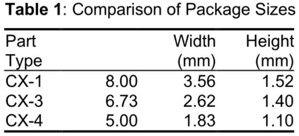
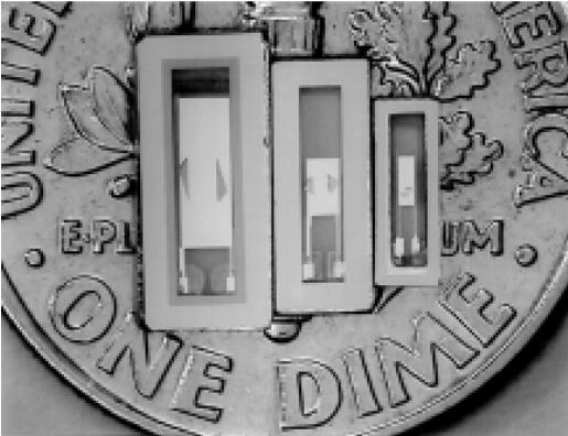
Figure 1: Three-size AT-strip resonator. From left to right: CX-1, CX-3 and CX-4.
A typical ultra-small AT blank is approximately 3.50 mm x 0.63 mm. Due to the small size, a tolerance of 2 μm is required in order to achieve an acceptable yield. Although conventional machining techniques cannot meet this stringent tolerance requirement, the photolithography process maintains dimensional tolerances better than 1 μm.
The lithography process begins with a polished quartz wafer (1 inch by 1 inch or larger).
These wafers were chemically etched to a predetermined frequency using an electron beam vacuum deposition system, cleaned and metallized with a film of chromium and gold. (Other metals, such as aluminum or silver can be used.) The AT stripe pattern is created by photolithographic techniques using a mask and a double aligner, where the top and bottom surfaces of the wafer are simultaneously aligned and exposed. The crystal electrode and probe pad pattern are then defined by subsequent photomask steps. The wafer is then chemically etched with metal and quartz to form individual AT strips. Finally, the top and bottom mounting pads are joined together using an aperture mask and thin film metal deposition [2].
Once the photolithography process is completed, our wafer will contain 125 separate ultra-small AT quartz crystal resonators, as shown in Figure 2. Each resonator is physically connected to the wafer by two small quartz tabs that also electrically connect the resonator to the probe pad on the wafer. This allows each resonator to be electrically tested while still on the wafer.
Frequency adjustment of physical and electrical properties of ultra-small low profile quartz crystal
Although the frequencies of the individual resonators on the wafer are very close to each other, the variation may be as high as 1%. This change is attributed to the non-uniformity of the thickness (wedge) of the wafer and, to a lesser extent, to the unevenness of the thickness of the metallization.
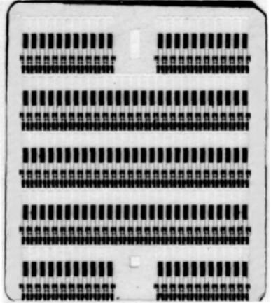
Figure 2: 125 ultra-small AT resonators on a quartz wafer
The frequency variation of the resonators on the wafer is considered in its production, so each resonator is now above the desired final frequency.
Then, using a wafer backplane, a gold film is deposited on the electrodes of each resonator to reduce its frequency to the final frequency [1].
The purpose and concept of the wafer backplane is similar to the conventional backplane of a quartz crystal resonator in a package, that is, by depositing gold to control the frequency reduction. The key difference is that the positioning in the wafer backplane system is much more precise. In the case where the resonator is already in the package, the accuracy with which the backplate can be applied to the quartz crystal resonator is limited by the accuracy with which the resonator can be placed in the package (unless an image recognition system is used). In the case where the quartz crystal resonator is still on the wafer, the position of each resonator is fixed and known.
Furthermore, although in both cases gold is deposited on the electrodes of the resonator through a series of holes, in the wafer backsheet, the holes that expose the electrodes of the resonator to the gold spray are themselves quartz wafers, The manufacturing process is the same as that of quartz - a crystal wafer, and uses the same mask pattern as the crystal wafer.
Therefore, the size and tolerance of the aperture wafer are the same as those of the crystal wafer, and the alignment of both is better than 25 μm.
Since the position of each resonator on the wafer is fixed and known, the wafer back plating system can detect each resonator using a probe pad on the wafer and then automatically separate each resonance. The backboard is carried out.
After adjusting all of the resonators on the wafer to the desired frequency, each resonator is removed and mounted in a ceramic package. This is done using a semi-automated assembly device that rushes out of the wafer and picks up the crystal while dispensing a conductive epoxy on the crystal package.
The crystal is then placed and placed in a crystal encapsulation chamber. (See Figure 3.) The unassembled patch crystal is then sealed using a matching glass or ceramic cover.
Electrical characteristics of ultra-small low profile quartz crystal oscillator
Recall that the isolation mode of the crystal is electrically modeled as a parallel combination of capacitor C 0 and inductor L 1 , capacitor C 1 and resistor R 1 . The difference is that the difference between an ultra-small AT crystal and a larger brethren is a larger series resistance R 1 and a smaller series capacitance C 1 (both due to the smaller area of ??the electrode [3]). In Table 2, we present the electrical parameters of three CX-4 AT crystals at three different frequencies. Using these values ??to calculate the value of their larger CX-1 counterpart (not shown here), we find that R 1 is about 2 to 3 times the resistance of its larger CX-1 counterpart, while C 1 is approximately It is a value of one-half to one-third of CX-1.
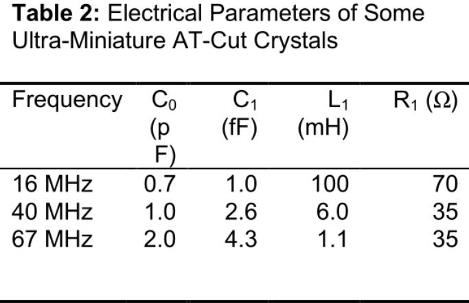
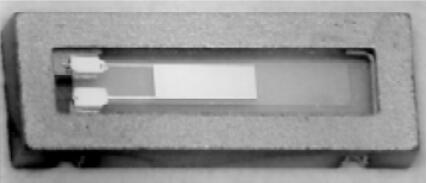
Figure 3: Ultra-small AT crystal resonator in CX-4 package (before sealing).
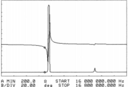
It can be seen in the impedance scan of the ultra-miniature crystal in Fig. 4 that such small crystals can achieve good electrical performance because their basic modes are completely separated from other modes.
In a frequency band of approximately 5% of the fundamental frequency of the crystal, only one non-harmonic mode is visible. The resistance of this mode is high enough and far enough away from the main mode (in frequency) that the effect is negligible.
正在載入評論數據...
相關資訊
- [2026-02-06]艾博康Abracon在推出電子商務功能,實現...
- [2025-09-18]Geyer晶振賦能極端環境下科技的堅守
- [2025-06-24]Greenray插件YH1300恒溫晶振OCXO的輸出...
- [2024-03-14]RTV119系列性能超強的溫補晶振由安德森...
- [2024-03-14]IQD最新推出IQXC-26系列體積超小耐輻射...
- [2024-03-12]Pletronics晶振最新推出的OSN4系列恒溫...
- [2024-03-08]回顧Bliley晶振八十多年的歷史進程
- [2024-03-08]Bliley如何測量并減少晶振老化帶來的影...
- [2024-03-07]Crystek行業標桿壓控晶振CVCO33BE-2352...
- [2023-09-28]遙遙領先的GEYER晶振跟大家一起探討尺寸...
- [2023-09-26]領先全球的HELE晶振帶你了解從原始石英...
- [2023-09-23]領先全球的Renesas Electronics Corpor...

 銷售代表
銷售代表 售后服務
售后服務

